Building a multi purpose EMI filter from scratch
Last year I stumbled upon a very interesting schematic of a multipurpose filter on the forum diyaudio.com and I decided to turn it into a useful, easy to manufacture PCB to be used in all sort of sensitive audio and electronic applications.
The primary function of an EMI filter is to block (or attenuate) any noise and electromagnetic interference produced by the device plugged after the filter AND any noise and interference going to the device from the power outlet, so it’s a bidirectional job.
We will see that this filter does more than just filtering, it adds protection to any device connected to its ends.
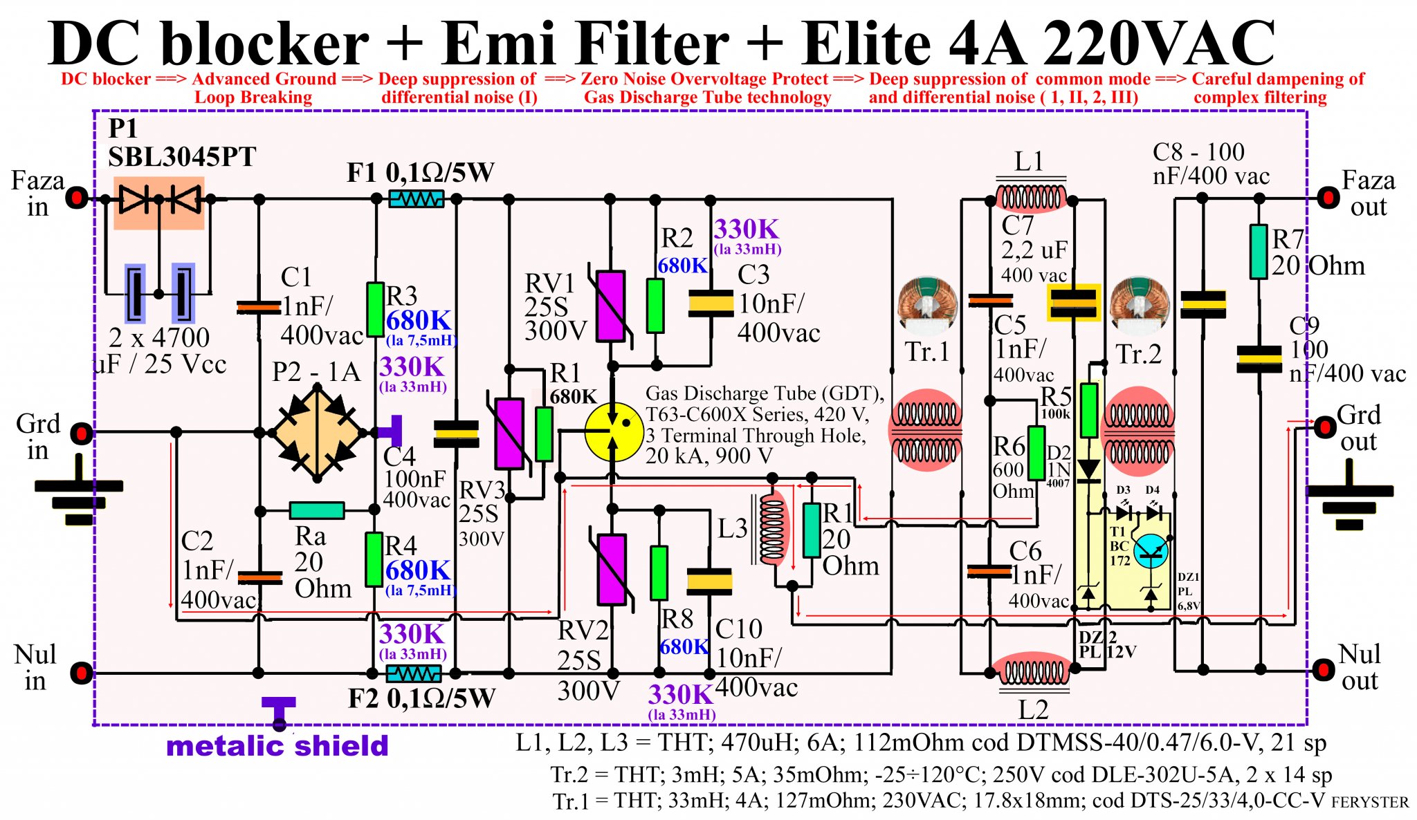
What follows is my version of the EMI filter, with explanation of some of the blocks/parts. I didn’t follow the original circuit 1:1, I used it as a base and concept and then adapted it using common components (primarily sourced from TME.eu and Aliexpress.com, so very easy to find).
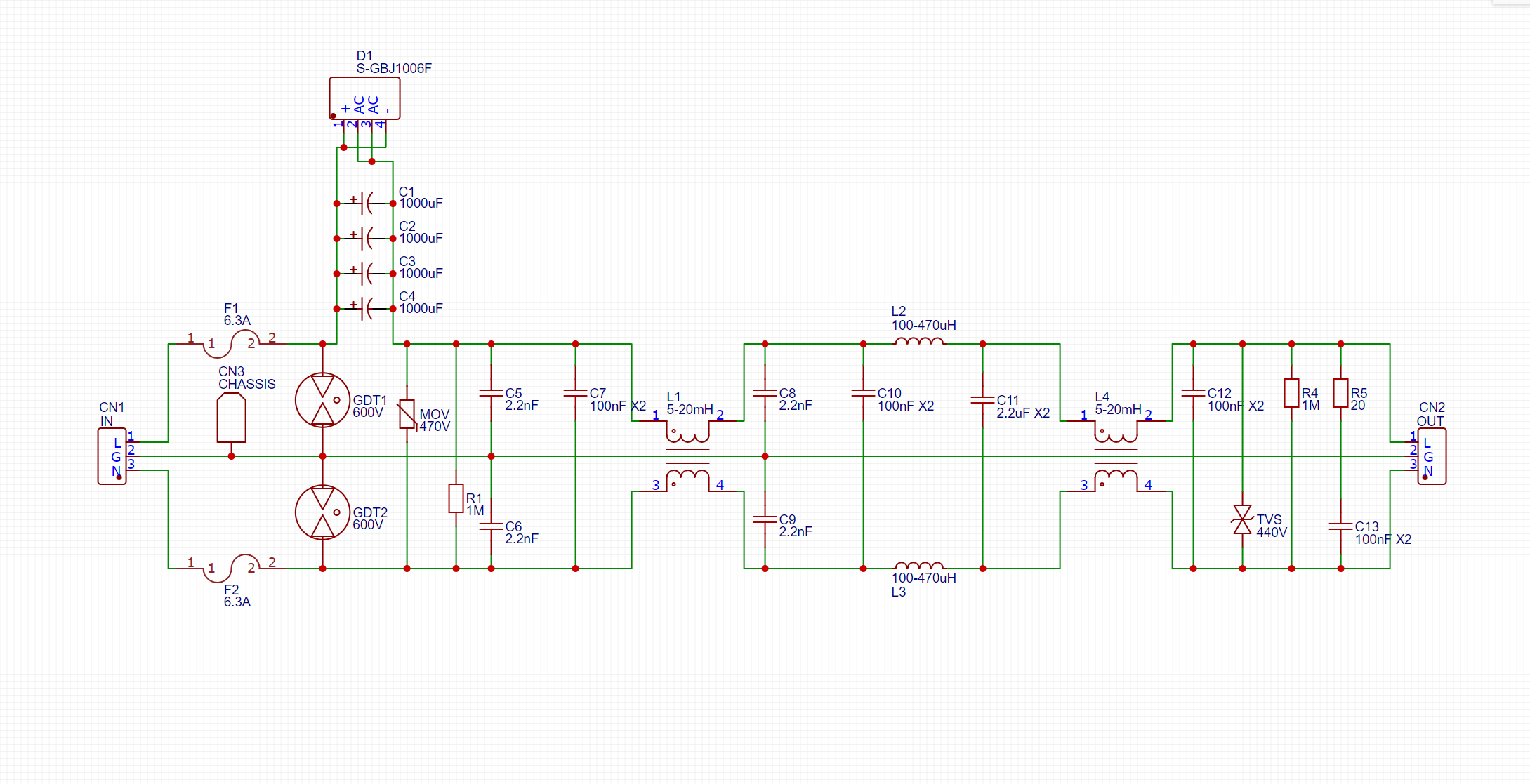
- CN1: input power connection;
- F1, F2: two fuses, we don’t know for sure if LIVE and NEUTRAL are connected in the right order when the filter is mounted by any user, so it is safer to put a fuse on both;
- GDT1, GDT2: gas discharge tubes, they are useful in case of a lightning strike or a voltage spike on the input. They short circuit when they reach a threshold voltage, blowing the fuses and preventing any unwanted spike to reach the output of the filter;
- The section made by the bridge rectifier D1 and the capacitors C1, C2, C3, C4 simply allows AC current to transit but blocks any DC current lower than 0.7-1V, providing a shield against DC pollution that may be present on the line (usually within a few millivolts);
- MOV: another safety component (with faster response time than the GDT) protects against surges by acting like a very low resistance resistor when the threshold voltage is reached, blowing the fuses;
- What follows is a standard EMI filter with two common mode inductors L1, L4 (which block common mode noise), two normal inductors L2, L3 (which block differential mode noise);
- The Y type capacitors C5, C6, C8, C9 are all part of the differential filter, connecting the power lines to Earth and filtering high frequency noise;
- The X type capacitors C7, C10, C11, C12, C13 are all part of the common mode filter, connected directly between the power lines filtering noise and providing help against voltage spikes;
- Some safety bleeding resistors R1, R4 to safely discharge all the charged capacitors when the filter is unplugged;
- Last but not least the TVS, it is connected directly to the output of the filter and suppresses high voltage spikes coming from any high power inductor or transformer connected to the filter during its operation/turn on.
After analyzing all the components of the filter we can move to the PCB design and component placement. The goal I had was to get whatever cheap enclosure I could find online and then shape the circuit board in order for it to fit inside of it.
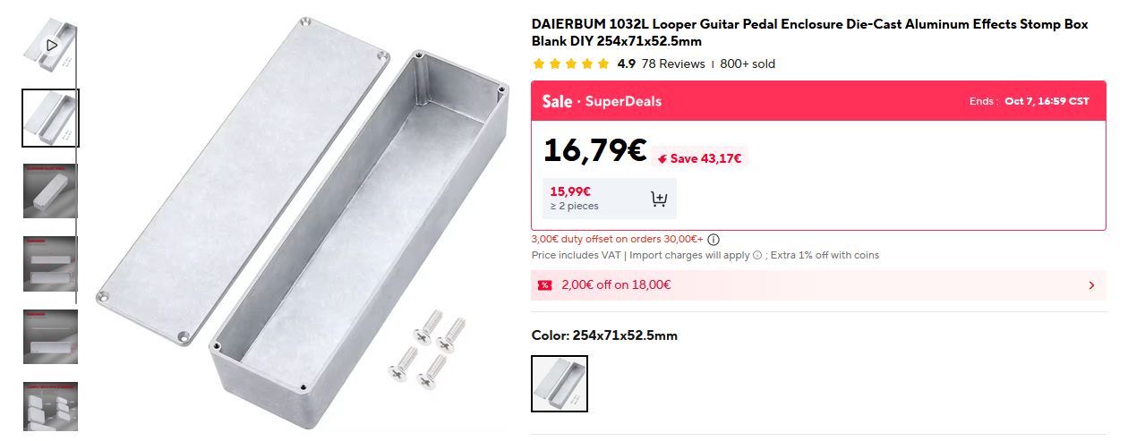
After acquiring the enclosure I took measures of it and made a basic shape that could fit in the enclosure, still maintaining an adequate safety distance from the walls to prevent voltage arcs. Then arranged all the components in a straight line, keeping the order as much as possible close to the schematic, and using two wide traces for power and a smaller one for earth (PE).
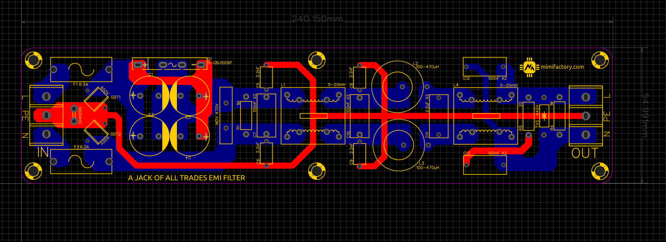
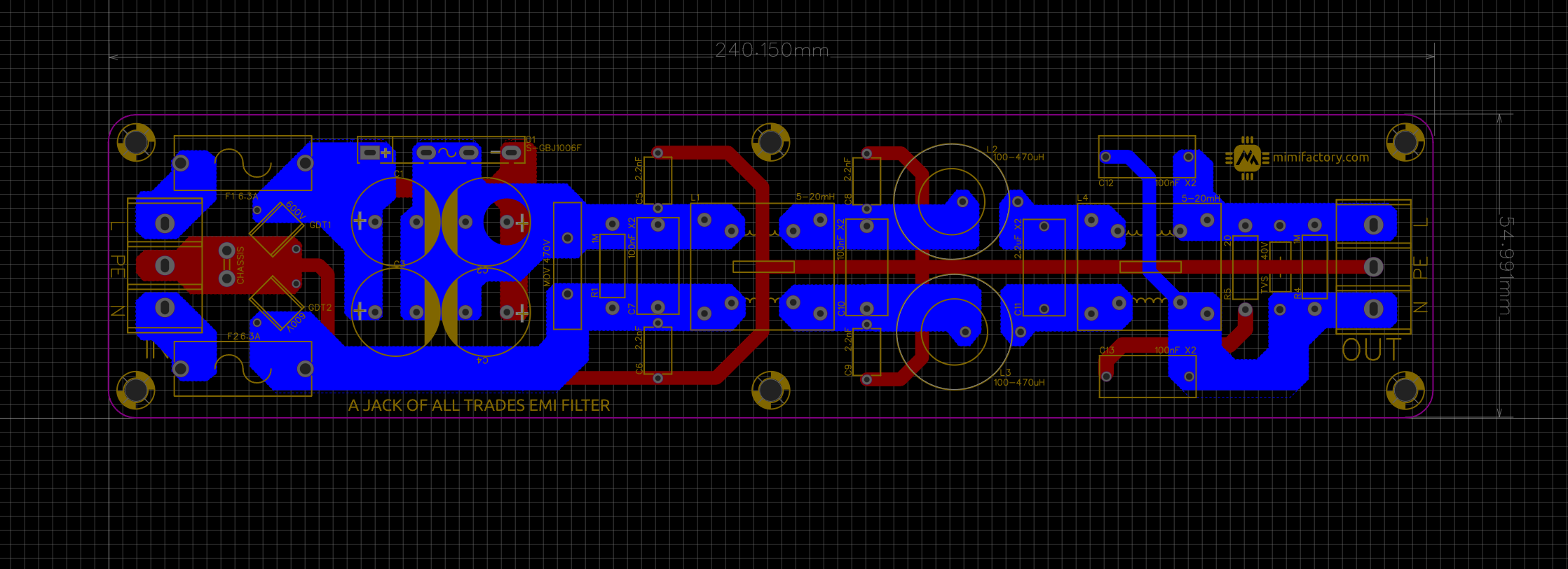
I made sure to keep a safety distance of 5mm to edge of the board and 4.5mm between the main voltage traces, above the 2.5mm distance required by IPC-2221. What follows is the normal routine of generating Gerber files and sending it to the fabricator, then soldering the components on the board.
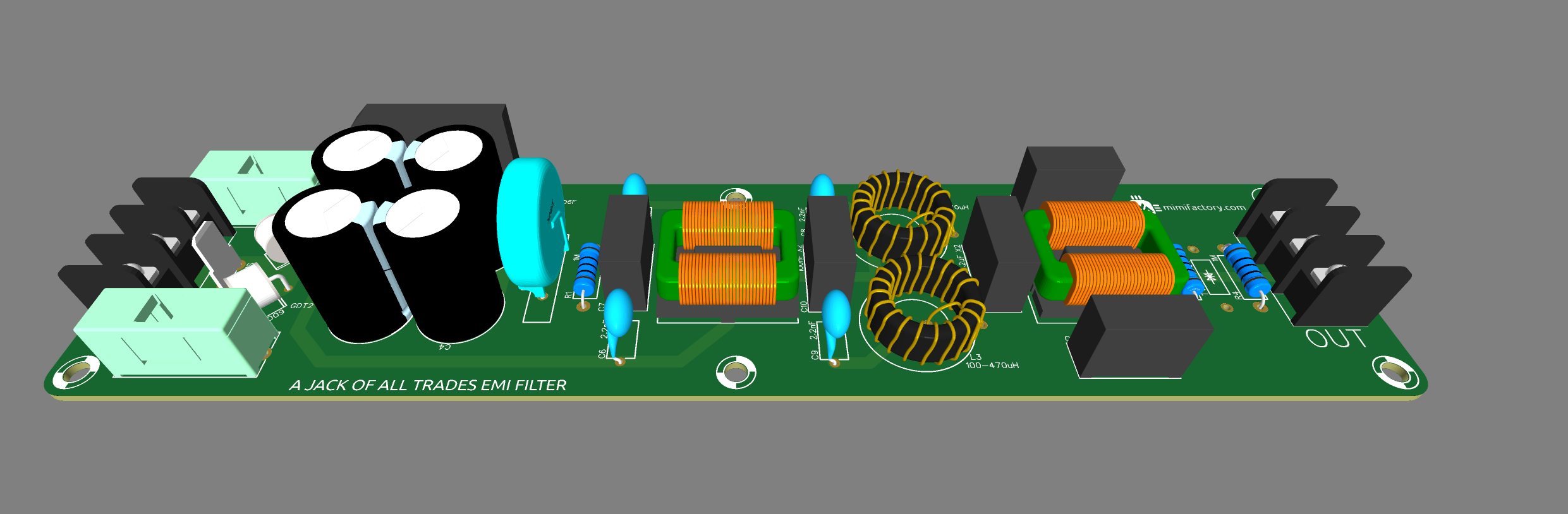
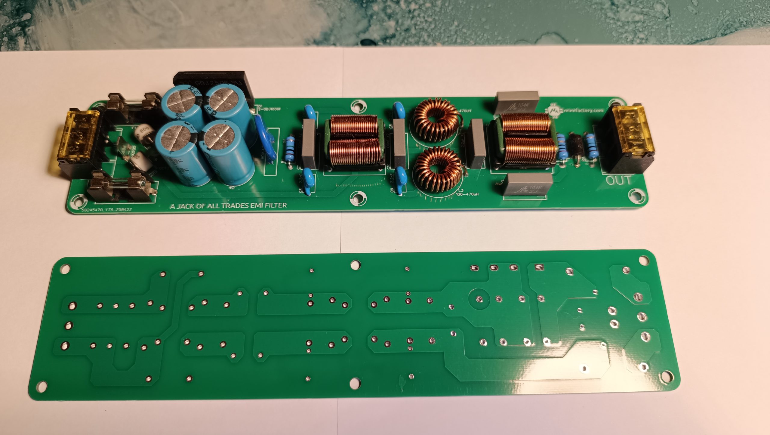
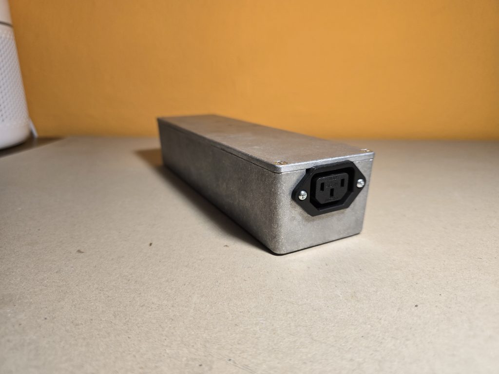
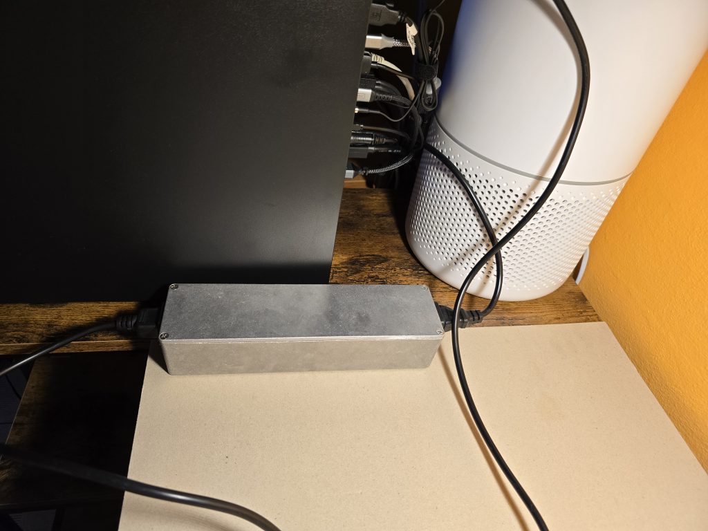
I soon realized that I needed a way to connect the filter to my devices and to the power outlet, so I adapted the enclosure to fit two IEC plugs (male and female) In the following gallery I illustrate the process of mounting the PCB inside the chassis and attaching the power plugs.
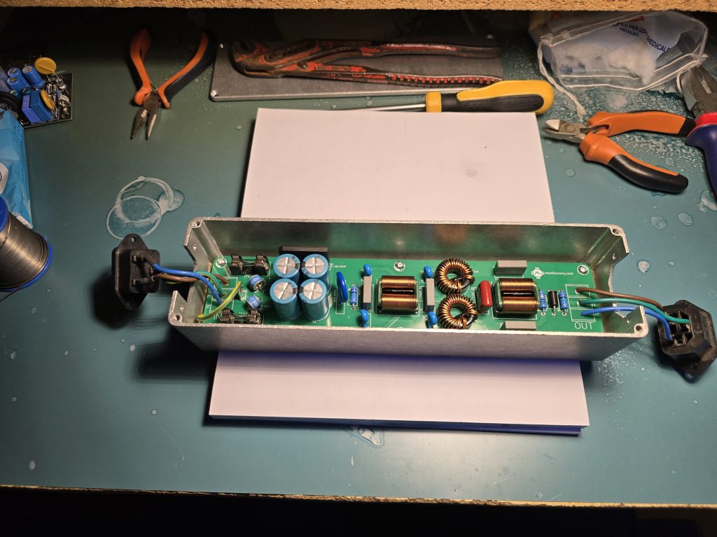
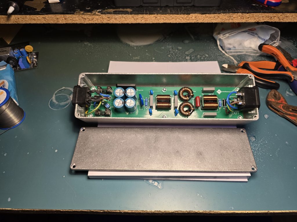
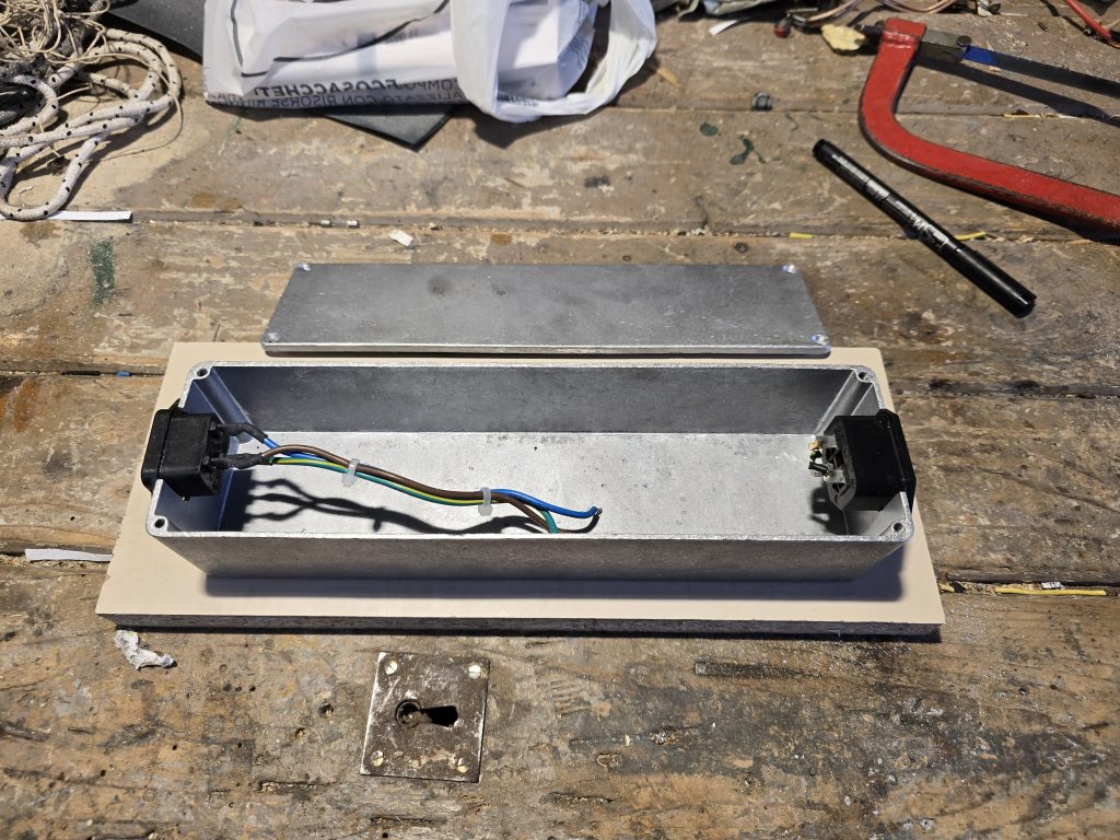
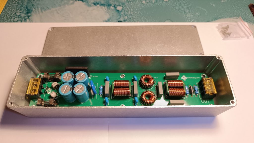
The filter now lives behind my PC, and it has been working without issues for over 6 months now.
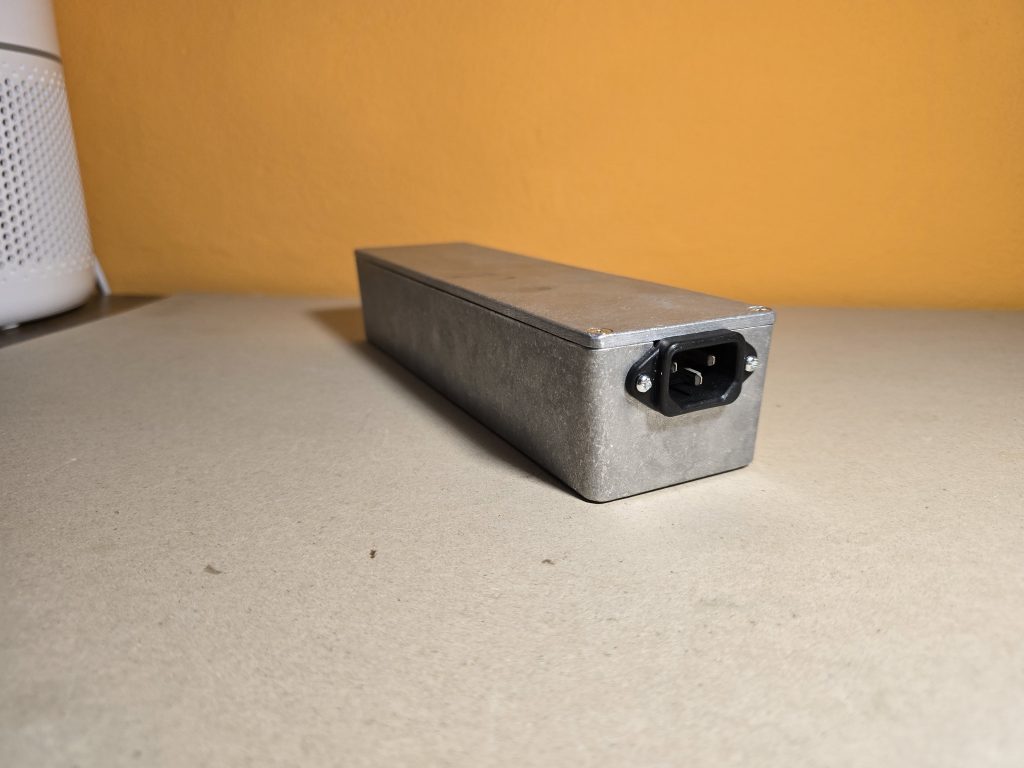
List of components used in the filter:
- 1 x DAIERBUM 1032L Looper Guitar Pedal Enclosure
- 2 x Terminal Block 7.62mm 3pin
- 2 x SQ2418 5mH common mode inductor, horizontal
- 2 x Toroidal Core Inductors 65125 68uH
- 2 x ESKA ZH10-G Fuse Holder
- 2 x TDK B88069X2880S102 Gas Discharge Tube
- 1 x MOV B72220S0301K101
- 4 x CC2820KY5P1KVB5LS-LF 82pF 1000V capacitor
- 1 x TVS 1.5KE440CA
- 4 x LE1H102ML250A00CE0 1000uF 50VDC capacitor
- 4 x MPEB-100N15/630 100nF 630VDC capacitor
- 1 x ECW-FD2J225 630VDC 2.2uF capacitor
- 2 x MF02SJJ0105A10 1MOhm 2W resistor
- 1 x MF02SFF200JA10 20Ohm 2W resistor
- 1 x GBJ1006F bridge rectifier
Gerber files of the project to download:

Post Comment